
The development of new technologies in power electronics has directed the industrial market towards other resources to optimize energy efficiency. Silicon and germanium are two of the main materials used today to produce semiconductors. The limited development in terms of losses and switching speed has directed technology towards new wide-bandgap resources such as silicon carbide (SiC).
SiC offers a higher efficiency level than silicon, mainly due to significantly lower energy loss and reverse charge. This leads to more switching power and less energy required in the switch-on and switch-off phase. Lower heat loss also makes it possible to remove cooling systems, thus reducing space, weight and infrastructure cost. With the growing deployment of IoT and AI applications and the migration to the cloud, a higher level of efficiency in the management of energy-intensive IT infrastructure will become increasingly important.
Silicon carbide has a wider bandwidth than pure silicon, this allows technology to be used even at high operating temperatures.
Wide-bandgap parameters
Wide-bandgap semiconductors have much wider bandgap than common semiconductors such as silicon or gallium arsenide (GaAs). This naturally translates into a greater breakdown electric field and into the possibility of operating at high temperatures and reducing radiation susceptibility without losing electrical characteristics.
As the temperature increases, the thermal energy of the electrons in the valence band also increases until they reach the necessary energy (at a certain temperature) to jump to the conduction band. In the case of silicon, this temperature is about 150°C; in the case of WBG semiconductors, however, these values are much higher.
A high electric breakdown field offers a higher breakdown voltage. This voltage is the value at which the breakdown body diode is broken, and an ever-increasing current is flowing between source and drain. The breakdown voltage of a PN junction diode is proportional to the breakdown electric field, while it is inversely proportional to the concentration of the material.
The high electric field offers excellent levels of doping and resistance of the much lower drift regions. With the same breakdown voltage, width of the drift region is inversely proportional to the breakdown electric field.
Another important parameter is the on-resistance of the drift region. Analyzing the previous example of a PN junction diode, we can see the on-resistance is inversely proportional to the breakdown electric field for a unipolar component.
The thinner semiconductor layers involve a lower density of minority charge carriers, an important parameter for defining the reverse recovery current. In fact, with other characteristics being equal, a component with a larger die designed to support higher currents will have a larger charge that undergoes the transient between conduction and interdiction and, therefore, will have a larger reverse recovery current. The ability of a semiconductor to switch to high frequency is directly proportional to its saturation drift speed: the drift speed of silicon carbide and gallium nitride is twice that of silicon. As a result, the latter can safely operate at higher frequencies. Also, a higher saturation drift rate is equivalent to faster removal of charges; this results in a shorter recovery time and a lower reverse recovery current.
The possibility of operating at high temperatures and a wider band gap also depends on the thermal conductivity of the material. There are several ways to evaluate thermal resistance: you can analyze the thermal resistance between junction and case or the thermal resistance between junction and environment.
The thermal resistance between junction and environment is a useful parameter when external heat sinks are not connected, for example in those cases where you want to compare the thermal performance of different packages.
It is possible to compare the materials using the figure of merit in a way that is proportional to the product between on-resistance and input charge at the gate. These parameters determine conduction and switching losses respectively and are connected to each other; usually, a lower charge value component will have a slightly higher on-resistance.
SiC diodes
Silicon carbide diodes are mostly Schottky diodes. Classical silicon diodes are based on a P-N junction. In Schottky diodes, metal is substituted with the p-type semiconductor, creating a metal-semiconductor (m-s) junction or Schottky barrier. This offers a low conduction drop, high switching speed, and low noise. The Schottky diode is used to control the direction of current flow within a circuit, allowing it to only pass from the anode to the cathode. When a Schottky diode is in an unbiased state, the free electrons will move from the n-type semiconductor to the metal forming a barrier. In the case of a forward-biased state, electrons can cross the barrier if the voltage is greater than 0.2 V.
The leakage current of a silicon carbide diode is much lower than that of a normal diode. As a WBG semiconductor, silicon carbide has a much lower leakage current and can be doped much higher than silicon. In addition, the forward voltage of the SiC diode is higher than that of the silicon diode due to the wider bandgap of silicon carbide.
In an interview with Amine Allouche, member of System Plus Consulting’s Power Electronics and Compound Semiconductors team, we highlighted some features of SiC diodes.
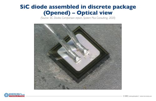
Unlike normal PiN diodes, Schottky diodes do not have recovery current because they are unipolar components with majority charge carriers. However, they do exhibit some recovery effects caused by the parasitic capabilities and inductances of the package and circuit. The main applications for SiC diodes are in power supply circuits but especially in PFC (Power Factor Correction) circuits in CCM (Continuous Conduction Mode). Silicon carbide (SiC) gives the diode a higher fault voltage and higher current capacity, thus finding room in industrial charging.
“According to Yole Développement, the power SiC bare diode die market was worth $160M in 2019. This includes various different market segments, such as automotive, energy, industrial… In fact, SiC diodes are mainly used in medium-voltage applications (automotive, PV, motor control…) to high-voltage applications (smart power grid…). In automotive applications, SiC devices, and particularly SiC diodes, are currently adopted in On-Board Chargers (OBC),” said Allouche.
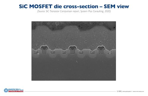
As with all SiC chips, Allouche highlighted that the main challenges faced by SiC diodes can be classified into three levels:
- Material level: SiC wafers have a high production cost (compared to Si wafer, for example). The commercialized wafer size is still limited (up-to 6-inch), whereas Si wafers are currently transitioning to 12-inch.
There is a limited number of high-volume suppliers of high-quality wafers, which are needed to manufacture a reliable device. This is highlighted in our report where we compared raw SiC wafer cost of the SiC diode manufacturers/sellers: Infineon, Wolfspeed, Rohm, STMicroelectronics, ON Semiconductor, Microsemi, and UnitedSiC.
- Device level: Device reliability is challenging with some critical process steps, such as SiC epitaxy, SiC doping (needs high temperature), SiC etching… Manufacturing yields still need to be improved compared to those of the more mature silicon technology.
The impact of epitaxy yield and wafer front-end manufacturing yield on the production cost of SiC diodes is detailed in our report.
- System level: Packaging is another challenge for SiC diodes. New packaging solutions need to be developed to fully benefit from SiC technology advantages. The different packaging aspects relevant to SiC diodes available on the market, from package type, die attach, to wire bonding, are detailed in Yole’s report.
SiC diodes can be assembled into discrete packaging, used as anti-parallel diodes with silicon-based transistors in hybrid modules, or as anti-parallel diodes in full SiC modules with SiC transistors.
“In our report, we highlight, for example, the die attach choices of manufacturers. Among the 11 SiC diodes by 7 manufacturers that we analyzed, we observed 5 types of die attach. Among them, Tin-based attach is the most common. However, one seller uses a specific type of high-performance die-attach, but this is to the detriment of manufacturing cost,” said Allouche
The high thermal conductivity of silicon carbide allows better heat dissipation, offering smaller form factors than silicon. This allows cutting on lower costs and having smaller packaging.
Recovery time and electrical recovery charge are shallow in silicon carbide Schottky diodes; the essential and interesting thing is that recovery time and current are independent of temperature and current transients, unlike silicon diodes where recovery time and current increase greatly with temperature.
SiC diodes are an excellent replacement in inverters: by simply using them as diodes to be placed in antiparallel to silicon IGBTs, it is possible to reduce losses. In a typical hybrid electric vehicle (HEV), replacing silicon components with silicon carbide components increases the traction efficiency by more than 10%. This results in a reduction of the heat sink volume to 1/3.