
At “Advancements in Thermal Management 2021,” an event that was held entirely online, three major experts on GaN and SiC technologies provided invaluable information about thermal models, packaging, thermal analysis, and thermal interface material techniques.
Proper thermal management of electronic components and circuits is a fundamental requirement to ensure the correct operation and reliability of the system in all operating conditions. The current trend toward a progressive miniaturization of electronic devices, followed by the increasing demand for power density, puts the issue of thermal management in the foreground, especially for the latest-generation power devices, such as those made from gallium nitride (GaN) and silicon carbide (SiC). GaN- and SiC-based devices can provide the high performance required in the latest-generation power applications. However, their extremely high power densities should be properly managed, making innovative thermal management techniques a crucial aspect to consider.
To fully exploit the potential offered by wide-bandgap (WBG) semiconductors, designers must understand the challenges that the use of these materials impose. Operating at higher switching frequencies and at higher power density, it is possible to achieve a size reduction of passive components (inductors and capacitors) and to fabricate lighter and smaller systems. However, the behavior of these smaller passive components working at higher frequencies is difficult to predict, and thermal management issues could arise. WBG semiconductors require careful design, as they operate at higher temperatures compared with those supported by silicon-based devices. The design process considers greater thermal stresses, which can adversely affect the reliability of the system. One of the biggest challenges for electronic designers is to reproduce or simulate severe operating conditions in which electronic devices are subjected to high thermal stress.
At “Advancements in Thermal Management 2021,” an event that was held entirely online, three major experts on GaN and SiC technologies provided invaluable information about thermal models, packaging, thermal analysis, and thermal interface material techniques. The panel was moderated by Maurizio Di Paolo Emilio, editor-in-chief of Power Electronics News, and hosted industry luminaries from major companies such as Efficient Power Conversion (EPC), UnitedSiC, and STMicroelectronics.
EPC
Alex Lidow, CEO and co-founder of EPC, started the talk by mentioning the thermal management of chip-scale GaN. According to Lidow, EPC GaN-based power devices have been in production for about 11 years. During the talk, he said that because GaN devices are so much smaller than the power MOSFETs they replaced (5× to 10× smaller), a common misconception is that they pose thermal management issues. Surprisingly, they are 5× to 10× more efficient in getting the heat out. Let’s consider the thermal resistance of a device going into a PC board. Lidow said that these devices are mounted facedown (flip chip), with all the active elements on the surface of the device, and they are really close to the PC board. The thermal resistance from the device junction to the bottom of the solder bumps (RθJB), having the same surface, does not differ much between silicon and GaN. However, as Lidow said, if we consider the opposite direction — the thermal resistance from the junction to the case (RθJC), or the thermal resistance out of the device either through the sidewalls or the back surface — it shows that GaN is about 6× more thermally efficient than silicon devices with the same dice area. Therefore, it is very common to see the devices on a PC board being placed face-down. These results can be achieved by placing a thermal insulating layer between the GaN-based power devices and a heatsink, as shown in Figure 1.
“There has been a lot of improvement in thermal insulating materials and gels; in just a couple of years, we’ve gone from about 6 W/mK all the way up to about 17 W/mK,” said Lidow. “Our solution allows not only heat conduction from the PC board up to the heatsink, but it also allows heat conduction out of the side of the device so that you get an even greater benefit by sidewall cooling.”
Lidow commented that simulation performed on a 4-mm2 representative device has shown what EPC has been able to confirm and achieve experimentally. In particular, better thermal management has been able to reduce the thermal resistance to about 3.9°C/W at 6-W power dissipation.
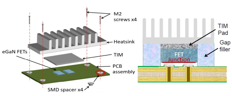
Figure 1: Reduction of junction to case thermal resistance
“We have a tool available to customers that allows designers to thermally model the entire system,” said Lidow. “Various elements can be configured, such as the gap filler, the thermal insulating pad, the heat spreader, the heatsink, and thermal vias.”
UnitedSiC
Jonathan Dodge, principal applications engineer at UnitedSiC, gave a talk about the trends in thermal management, with considerations about SiC. As Dodge said, the reduction of the on-resistance is definitely a trend that will continue over the next few years, and that will open up some interesting applications that otherwise would not really be handled by power semiconductors. “So we are also getting an increase in power handling per discrete device,” said Dodge.
“Silicon carbide allows reduced chip size, but the power per unit area of the chip is still relevant, meaning that we are relying more on the package and on the heatsink to provide thermal mass,” he added.
During his talk, Dodge highlighted two application branches posing tough design challenges regarding thermal management. The first one includes solid-state circuit breakers and relays with passive cooling, while the other one includes high-power converters and motor drives, which require more aggressive cooling. Both applications need a package that can handle the required power levels. Widely used packages, such as the TO-247, come with severe limitations. Their pins are small, considering that in motor drive applications, we might run over 100 ARMS through them. Then, as shown in Figure 2, there is a wasted area, as the SiC chip area is relatively small, compared with the package, which is huge. Dodge commented that creepage and clearance distance is also another problem, as this package was not designed for the high voltages that we are working with now. That’s why many designers prefer a clip mount with a ceramic isolator, as the ceramic will not wear out.
“I think the trend for the future is actually going to be surface-mount: It’s low-cost, super-reliable, and either top-side– or bottom-side–cooled,” said Dodge. “We need isolating thermal interface material that can handle multiple surface-mount devices, 800 V and even higher, and compliance for small SMT assembly variations.”

STMicroelectronics
Salvatore Coffa, group vice president and general manager at STMicroelectronics, completed the session with a talk about thermal management techniques in power devices, with considerations about thermal management design for traction-inverter applications.
Coffa noted that whenever we talk about innovation in the performance of power devices, we see the evolution toward higher power density along with lower power and conduction loss. This is true with silicon and or even more so with WBG semiconductors like SiC and GaN.
“A path to innovation is not only the innovation in the front end, or the material or the structure or the device, but the role played by the package is more and more important,” said Coffa.
To achieve this in power modules for an EV powertrain, Coffa said that we need to achieve low static and dynamic losses, improve the thermal resistance Rth (junction to fluid), and optimize the tradeoff between cost, performance, and reliability in the final application.
Coffa argued that an approach to power-module package design is based on the simulation, using tools such as CAD/CAE modeling. This greatly helps because it takes into account the properties of the device, the losses, and the thermo-mechanical constraints. As shown in Figure 3, this approach analyzed by Coffa permits the estimation of product lifetimes, starting from an initial packaging design with relevant operating conditions, by means of theoretical models of power loss, thermo-mechanical issues, and other damage. Coffa added that the final packaging design results from iterating the flow according to the topological or morphological optimization approach. And all models must be previously calibrated and validated by experiments, even on different designs.
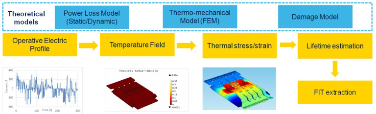
“We do a lot of CAD/CAE modeling, where we combine the electrical properties of the device with the properties of the thermal material, and we also do a lot of experimental work in order to select the proper parameter from the material that we use,” said Coffa.
SiC MOSFETs for electrical vehicle traction inverters require a proper co-design of the die and of the package, considering all the relevant thermo-mechanical aspects in the final applications. SiC power devices specifically conceived for the automotive domain are thought to often be mounted through non-conventional die-attach techniques. New SiC dice are particularly designed to be assembled through sintering, both on the bottom and on top for clip sintering. Sintering the dice on the active metal braze, or directly on the heat sink, exploits the exceptional electrical and thermal performance of this WBG material and provides superior reliability under temperature swing.