
Voltage references are key components in many electronic applications that include electronic instruments (e.g digital multimeters), analog to digital (ADC) and digital to analog (DAC) converters, linear and switched-mode power supplies as well in other linear integrated circuits.
Voltage references are key components in many electronic applications that include electronic instruments (e.g., digital multimeters), analog-to-digital and digital-to-analog converters, linear and switched-mode power supplies, and other linear integrated circuits.
In this article, we will focus on bandgap voltage references made by Texas Instruments, with a large selection of this particular form of voltage references.
Monolithic voltage references produce an output voltage, which is substantially immune to variations in ambient temperature as well as loading, input voltage supply, and time.
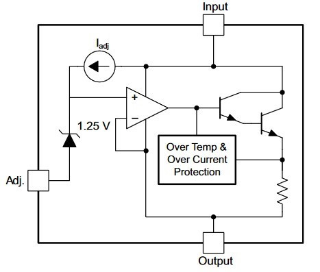
A bandgap voltage reference often is present in linear regulators like the LM317 shown in Figure 1.
The 78xx and 79yy series and a three-terminal adjustable, precision shunt voltage regulator integrated circuit, introduced in 1977 by Texas Instruments, the famous TL431 have one bandgap block, too.
In 1971, Robert J. Widlar, in its US patent number 3.617.859, proposed a novel approach to make a voltage reference based on two transistors having different emitter areas, used to generate an output voltage proportional to absolute temperature.
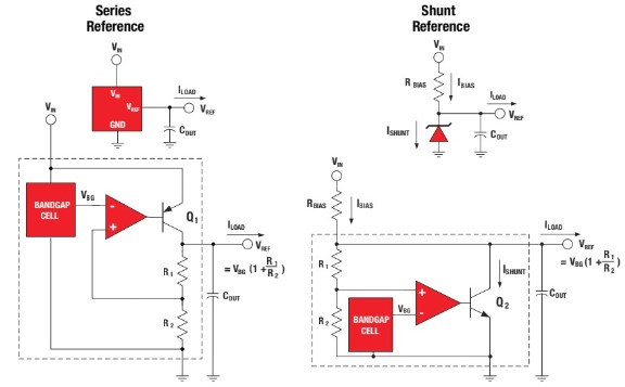
A bandgap voltage reference cell is at the heart of two main series and shunt topologies, as shown in Figure 2.
From the original Widlar’s patent, we can derive an equation for voltage reference (Figure 3).

Where:
- J1 and J2 are current densities
- VBE0 is the base-emitter voltage for absolute temperature T0
- Vg0 is the extrapolated energy bandgap voltage of the semiconductor material at absolute zero (i.e. 1.205 V)
- q is the electron charge 1.60217662 × 10⁻¹⁹ C
- k is the Boltzmann constant 1.38064852 × 10⁻²³ m2 kg s–2 K–1
The fundamental idea that Widlar used was to compensate the negative (–2 mV/K) temperature coefficient of the base emitter voltage VBE by summing it with a second voltage V(R2), which has a positive temperature coefficient.
Voltage reference specifications
1. Temperature coefficient
The variation of voltage reference over temperature is defined by its temperature coefficient (TC), which has units of parts per million per degree Celsius (ppm/°C).
Generally, the temperature coefficient can be expressed in polynomial form, as shown in Figure 4:

Figure 4: Temperature coefficient expression for bandgap voltage reference
where TC1 represents the first-order (linear) temperature dependence, TC2 the second order, and so on. The temperature coefficient can be specified over several different temperature ranges, including the commercial temperature range (0 to 70°C), the industrial temperature range (–40°C to 85°C), and the extended temperature range (–40°C to 125°C).
Texas Instruments’ REF32xx voltage reference series available in SOT23-6 package is specified for drift of 7 ppm/°C maximum at 0°C to 125°C and 20 ppm/°C at –40°C to 125°C. There are several methods to determine TC with the box method being used most often.
The box method calculates TC using the difference in the maximum and minimum VREF values over the entire temperature range, whereas other methods use the values of VREF at the endpoints of the temperature range (TMIN, TMAX).
With this method, a box is formed with min/max nominal output voltage over specified temperature range (Figure 5).

Texas Instruments’ LM4140 voltage reference exhibits a temperature coefficient of 3, 6, and 10 ppm/°C for A, B, and C grades.
2. Initial error
The initial error is the voltage value after the device is turned on and warmed up for a specified amount of time.
3. Initial accuracy and solder shift
The initial accuracy of voltage reference VREF shows how it is close to the stated nominal value at room temperature. For example, the LM4140 voltage reference is available with 0.1% initial accuracy and output voltage lower than bandgap voltage.
Another factor that affect the initial accuracy is called “solder shift” and involves a deviance from nominal voltage (@ 25°C) due to thermal shock experienced by voltage reference device. This thermal shock is caused by the soldering process itself and can’t be avoided.
4. Long-term stability
This parameter refers to the change of the output for a specified amount of time, usually 1,000 hours under nominal conditions. For Texas Instruments’ REF32XX series typical drift, the value is about 55 ppm for 0 to 1,000 hours.
5. Noise performance
Noise performance is the electrical noise superimposed in the output of a voltage reference. It can include thermal noise and narrowband 1/f noise. Wideband noise can be effectively filtered with simple RC network; the noise of 1/f type is specified over 0.1- to 10-Hz frequency range (peak to peak value). For example, the LM4040 offered from Texas Instruments has a wideband noise value of 35 µV RMS for a 2.5-V output.
5. Line regulation
Line regulation (Figure 6) is defined as a change in output voltage produced by a change in input voltage.

Power supply rejection ratio (PSRR) can be rarely included as a measure of how power supply voltage is noisy. Capacitors selected for low equivalent series resistance) can improve PSRR parameters.
6. Load regulation
Load regulation is a change in output voltage produced by a change in load current in parts per million (Figure 7).

7. Thermal hysteresis
Thermal hysteresis is a shifting in VREF value produced by one or more thermal excursions. The causes of thermal hysteresis include thermomechanically induced die stress due to temperature excursion, type of package, molding compound, die attach material, and the integrated circuit layout itself.
Thermal hysteresis for a LM4140 is 20 parts per million.
AD580, a three-terminal bandgap voltage reference
The Analog Devices AD580 (Figure 8) was a three-terminal, bandgap-based, voltage reference presented in 1974, also known as Brokaw cell.
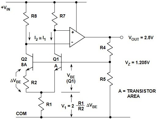
Figure 8: AD580
The AD580 has two 8:1 emitter scaled transistors Q2, Q1 operating at identical, collector currents. Bandgap voltage emerges at the base of Q1. Thanks to LASER trimmed R4 and R5 resistors, output value can be scaled to a voltage value that is different from that of a standard bandgap reference (e.g., 2.5, 5 VDC).
The LM113 from Robert J. Widlar
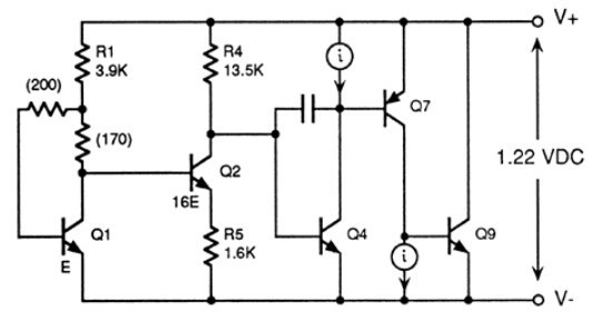
In 1971, Robert J. Widlar introduced the first bandgap voltage reference made by National Semiconductor and called it LM113 (Figure 9).
Temperature-compensated Zener diodes are the most easily used voltage reference. The lowest voltage attainable with a temperature-compensated Zener is 6.2 VDC. This makes it difficult to obtain a zero-temperature coefficient reference when the operating supply voltage is 6 VDC or lower.
The LM113 is a 1.2-VDC, temperature-compensated shunt regulator diode. The reference is synthesized using transistors and resistors rather than a noisy breakdown mechanism.
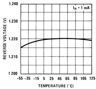
Figure 10 shows the typical change in output voltage over a –55°C to 125°C temperature range. The reference voltage changes less than 0.5% with temperature, and the temperature coefficient is relatively independent of operating current.
Conclusion
Voltage reference based on silicon bandgap voltage are fundamental blocks for every kind of analog integrated circuit. Bandgap references exhibit good initial accuracy, long-term stability, and low noise operations and are available with output voltages above the standard 1.25 VDC.
Bandgap references are also used in digital logic-like emitter coupled logic to provide a local bias voltage unaffected by temperature and ambient noise.
Also, SPICE models are commonly available for most integrated bandgap references in various packages (three terminal, DIP, etc.).