
In the typical configuration, a dual inverter is used to drive the two motors but it can also be used in back-to-back inverter topology to provide bidirectional power transmission.
Electric vehicles (EVs) and hybrid electric vehicles (HEVs) have grown in popularity as technology in the automobile industry has advanced (HEVs). The electrification process of the transportation system necessitates a large amount of power. Dual-inverter technology has been used to fulfill these requirements [2],[3]. There are two ways to use the dual inverter traction system. In the typical configuration, a dual inverter is used to drive the two motors but it can also be used in back-to-back inverter topology to provide bidirectional power transmission [1]. Fast switching, low switching losses and high power density have all been introduced with the invention of the WBG power devices and their use in the power inverter design [4],[5]. Due to their ability to operate at high temperatures, WBG devices such as SiC MOSFETs provide an additional benefit of a simple cooling system. However, because of the fast-switching speed, these devices have a high dv/dt and di/dt, which leads to electromagnetic interference and device failure [6],[7]. The inverter’s reliability is also influenced by the junction’s temperature rise. To overcome these drawbacks, an optimized inverter design is required.
The design of a SiC based 2x250kW dual inverter will be discussed in this article. We will also cover thermal analysis, new busbar design, dc link capacitor selection, and the impact of switching frequency on inverter performance [1]. The original article can be found here.
Designing the Busbar
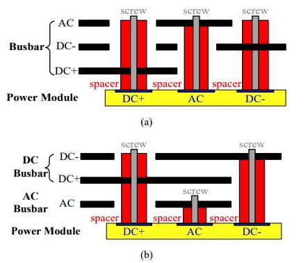
SiC MOSFETs are characterized by high switching frequency and low losses. The busbar design should be optimized to reduce stray inductance to support these characteristics. Figures 1(a) and (b) show the two busbar designs. In the first 3-layer busbar design, we can see that the laminated AC busbar is placed on top of the two DC bars. The advantage of this design is that the distance between the DC busbar and the power module is decreased but the laminated area is also reduced since the DC layer must maintain sufficient spacing from the AC busbar.
Figure 1(b) depicts the second busbar design, with the AC busbar at the bottom and the two DC busbars at the top. Although the distance between the power module and the DC busbar has increased in the second design, the laminated area has grown. The results show that increasing the lamination area results in less stray inductance, and when the two designs are compared, the second busbar design has 30% less stray inductance than the first.
Thermal Characteristics
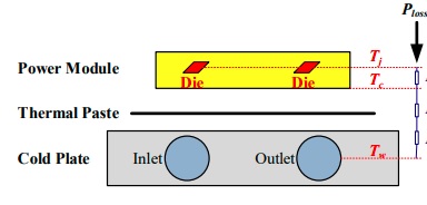
The junction temperature in power modules increases, due to conduction and switching losses, which have a significant impact on the inverter’s performance. As a result, it is critical to keep the junction temperature under control, which is limited to 175ºC. To keep the temperature below acceptable limits, a limited coolant is employed that runs via the cold plate bonded to the power module with thermal paste, as shown in figure 2.
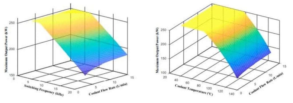
Figures 3(a) and (b) illustrate the inverter’s maximum output power at various coolant temperatures and switching frequencies. Figure 3(a) shows that the output power is highest when the coolant temperature is low and the flow rate is high, and it tends to decrease when the coolant temperature rises, or the flow rate decreases in the cold plate while the switching frequency is set to 20kHz. This is due to the cold plate’s increased thermal resistance [1]. Figure 3(b) depicts the output power at various switching frequencies and flow rates while the coolant temperature remains constant at 105 °C. As shown in the graph, a high switching frequency results in a low output power due to large switching losses. While a low switching frequency at a high coolant flow rate maximizes the inverter’s output power, it also causes ripples in the output, which has a detrimental impact on output quality.
Switching Frequency and DC link Capacitor
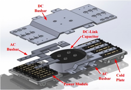
For high power density, HT-3000 series 1.2kV half bridge SiC modules [8],[9] are used in the proposed inverter architecture. The previously described optimized busbar design minimizes stray inductance and allows the inverter to support 250kW. As described in the thermal characteristics, the low switching frequency (5kHz) improves output power but degrades output quality because the low switching frequency causes ripples at the dc link and the output part of the inverter. A dc link capacitor is used to solve this issue. The coolant temperature is kept at 90ºC, and the flow rate is 3 liters per minute. Experiments have demonstrated that a low switching frequency results in a greater dc link capacitance, which not only increases the inverter’s cost but also affects its power density. On the other hand, a high switching frequency (20kHz) necessitates a small dc link size, resulting in a high-power density. So, in the suggested optimized inverter, the switching frequency is set at 20kHz, the coolant temperature is set at 90ºC, the flow rate is set at 3 liters per minute, and the power density is set at 60kW/L. Figure 4 depicts the dual inverter prototype. The parameters of the dual inverter are shown in the table below.

Conclusion
This article described the ideal design for a 2x250kW dual inverter. The busbar is built in such a way that stray inductance is minimized, allowing SiC MOSFETs to deliver lower switching losses. The thermal characteristics of the inverter and the effect of switching frequency on the inverter output are also discussed.