
When selecting a power supply it is essential to examine the voltage transient response specification and output impedance characteristics.
Today’s integrated circuits are operating faster than ever. The increased operating speed can lead to highly dynamic power demand from the power supply, which poses a challenge during testing when you source power using programmable power supplies. The high-speed current waveforms can lead to voltage drops at the integrated circuit. If severe enough, the voltage drop can reset the microprocessor or cause anomalies in your test results. This article explains why the voltage drop occurs, offers several ways to achieve the lowest possible voltage drop by selecting optimal load leads and power supplies, and the use of local bypassing.
Selecting programmable power supplies
Traditionally, to achieve the best possible output voltage regulation, you would use a linear power supply. However, linear power supplies tend to be very large, expensive, and highly inefficient at higher current levels. Recent advances in switching power supply technology make it possible to replace linear power supplies with switching power supplies in performance applications. Switching power supply designers face seemingly contradictory goals of low output noise, fast transient response, low cost, and high density. Achieving low output noise is usually accomplished with multiple stages of filtering or using larger filter components, both of which lead to higher cost, lower power density, and slower transient response. More advanced power supplies employ higher switching frequency, better filter design, and more sophisticated control topologies to optimize all the criteria. When selecting a power supply for IC test applications, it is essential to examine the voltage transient response specification and output impedance characteristics to ensure good performance.
Optimizing load wiring
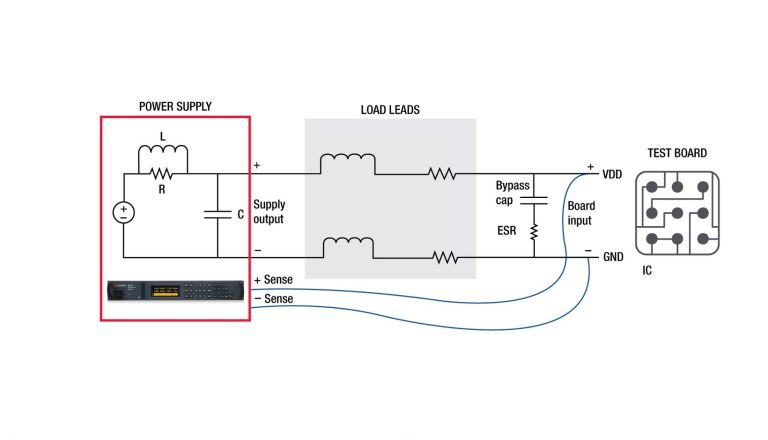
In many cases, physical constraints force you to position the power supply several feet away from your IC test board, necessitating at least a few feet of load lead wiring. Load lead wiring impedance can very quickly degrade the source impedance experienced by the IC. Almost all programmable power supplies provide sense lead inputs, which allow you to select the point of voltage regulation by connecting the voltage sense leads at that location. In this application, the sense point would be as close as possible to the IC. However, the voltage regulation loop can suppress voltage transients at this sense point only within its control bandwidth. Consequently, a voltage transient can occur at this sense point if the current transient rise time is sufficiently fast. Load lead impedance at these lower frequencies can be modeled as a lumped series inductance and resistance, as shown in Figure 1.
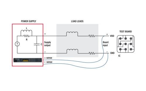
Let’s examine a 25-A application with 5-A transients in which the power supply is set to 2.5 V and connected to the IC test board via 5 feet of 14-AWG wiring. Because this is a low-voltage application, voltage undershoots greater than 100 mV are generally not acceptable. The 14-AWG wiring has 2.5 mΩ of resistance per foot, resulting in 25 mΩ of resistance for the round-trip connection between the power supply’s output and the IC test board.

The power supply voltage control loop will compensate the calculated 125-mV drop after a period commensurate with its bandwidth. However, in the meantime, the IC will experience this 125-mV voltage drop. In this application, the effect of the load lead resistance alone is enough to cause an unacceptable short-duration drop at the test board. However, the load lead inductance is another major cause of voltage drop. It is not uncommon for the test board to ramp the 5-A transient in a matter of 10 µs. This high rate of current change can cause a constant voltage drop across the leads during the current ramp. Load lead inductance changes based on the position of the positive and negative lead. Using an approximation of the inductance, you can estimate the voltage drop. In most cases, a 250-nH/foot inductor is a good model for non-twisted load wiring.
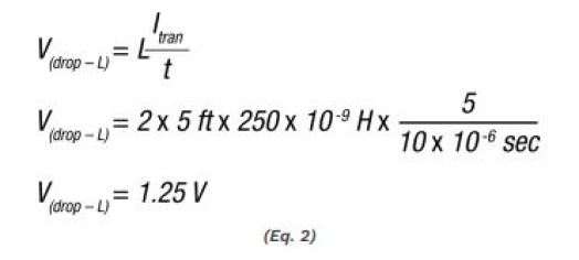
Combining the effect of the resistance and inductance in the leads, we get:
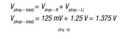
The result of 1.375 V is not acceptable. As mentioned previously, the power supply’s voltage-regulation loop will sense this voltage transient and adjusts the supply’s output by the necessary amount to maintain a steady 2.5 V at the test board. However, this process can take up to 1 ms, even with a good-performance power supply. To reduce the lead inductance effect, tightly couple the force leads together by either tying them together at regular intervals or by simply twisting them together. Twisting the leads also provides the added benefit of better immunity to other magnetic fields that may be present due to different load leads carrying large current transients. A good model for twisted leads is a 170-nH/ft inductor. This inductor includes both the positive and negative lead inductance effects. Recalculation with twisted leads yields:

Although the voltage drop has improved, the total result is not yet acceptable. Further improvement can be made by paralleling cable runs. For example, paralleling four sets of twisted cables will reduce the resistance and inductance by a factor of 4.

The goal of 100 mV is still out of reach, especially when we consider that the power supply will contribute additional transient voltage drop in response to the change in output current. More specialized cabling options such as custom coaxial cables or flat-wire cables can improve the inductance effect to as low as 10 nH/ft. However, these options are costly and not as readily available. An alternative is low-impedance energy storage located very close to the test board.
Using a local bypass capacitor
The power supply cannot compensate for the voltage drop across load leads and the drop across its output rapidly enough, so you need a local source of energy, as shown in Figure 2. Capacitors are well suited to provide low impedance at high frequencies to compliment the low impedance provided at low frequencies by the power supply. Many different capacitor technologies are available and finding the right part or a combination of components can be difficult. Ceramic capacitors are well suited for providing high-frequency bypassing at low voltages. However, even with the recent advances in ceramic capacitor technologies, they cannot match the high density and low price of aluminum electrolytic and conductive polymer aluminum solid electrolytic capacitors. The equivalent series resistance of the bypass network is an essential parameter, as it appears in series with the capacitor and can significantly reduce the effectiveness of the bypass network. Selecting the lowest necessary voltage capacitor will help you obtain the lowest-ESR capacitor and the highest capacitance density.
The interaction between the power supply voltage control loop, the load lead network, and the bypass capacitance can be a bit complex. However, some simple approximations can help you with the initial value selection for the capacitor. The process is as follows:
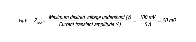
1. Calculate the peak network impedance. Determine the desired peak impedance of the load lead network and bypass capacitance by using the following expression:
2. Calculate the bypass capacitance value. Set the desired peak impedance equal to the expression for the characteristic impedance of the L-C tank formed by the load lead inductance and the bypass capacitance. Solve the expression for the value of capacitance:
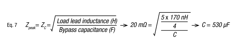
3. Calculate the resonant frequency of the tank. The power supply you use must have lower output impedance than the characteristic impedance of the L-C tank; otherwise, the calculation you perform will not properly predict system behavior. The power supply output impedance will decrease with decreasing frequency. In a case where the power supply output impedance is higher than the desired peak impedance, pick a tank resonant frequency to equal the frequency at which the power supply output impedance is less than or equal to Zpeak. The resonant frequency must be lowered by selecting a larger bypass capacitor.

4. Select the desired capacitor ESR to ensure proper damping of the L-C tank. Proper damping of the resonant tank is crucial, as an improperly damped tank will tend to ring and can also have a destabilizing effect on the power supply control loop. The combination of the load lead resistance and capacitor ESR will work to damp the resonant tank. We will target a damping ratio of 0.5 for faster response and lower peak voltage by equating the tank resistance to the L-C tank’s characteristic impedance.
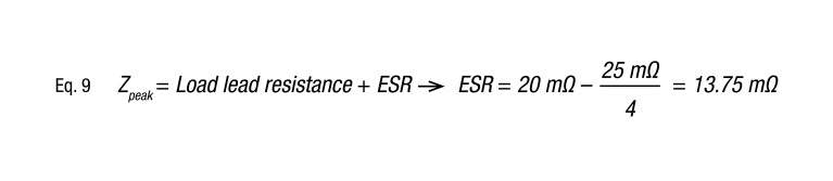
Because it may not be possible to find one capacitor with the right capacitance and ESR, you can use parallel combinations of capacitors with different values and ESRs to arrive at the desired parameters.
Results
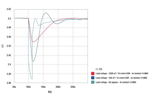
Figure 3 shows the transient voltage response observed at the load when using the Keysight N7950A dynamic DC power supply. It is ideal for low-voltage, high-current operation and very low output impedance, which is perfect for this application. The light blue trace represents the four twisted pairs of cables without a local capacitor. Dark blue is the response from adding a 530-µF capacitor, as calculated in Equation 7. Increasing the capacitance by 4× drops the tank impedance by a factor of 2 and yields the results shown in red.
Summary
This article explored the challenge of supplying a highly dynamic load with a stable voltage using a power supply located several feet away from the device under test. Although the load lead impedance can severely degrade the transient response performance of a high-performance power supply, with mitigation practices, you can achieve the required performance at the device under test. Techniques such as twisting load lead wiring to minimize the loop area formed between the supply and return lines, using flat copper, or heavy gauge coaxial cables can significantly reduce the load lead inductance. Properly sizing a bypass capacitor network at the device under test can further improve voltage-level stability in the face of fast current transients drawn by the device under test.