
Wafers are made of very pure material that, during the manufacturing process, must be polished to obtain a very even and smooth surface. This result can be achieved by applying lapping, polishing, and grinding techniques.
Semiconductors are among the most widely used components in electronic circuits, in which they guarantee reliability, high resistance, and low cost. The manufacturing process of semiconductor devices, commonly used to create integrated circuits, involves a sequence of multiple photographic and chemical processing steps, during which the electronic circuits are gradually created on a wafer of pure semiconductor material. Although silicon is still the most widely used semiconductor material, there are other semiconductors (such as wide-bandgap materials) that can offer superior performance to that of silicon.
Wafer-finishing solutions
Wafers, whose dimensions are gradually increasing and can reach 200 mm (8 inches), are made of very pure material which, during the manufacturing process, must be polished to obtain a very even and smooth surface. This result can be achieved by applying lapping, polishing, and grinding techniques. Lapping is a mechanical technique that removes extra silicon from a wafer substrate using a pad and polishing liquid, leaving a dull-gray, semi-reflective finish. Lapping helps to remove faults on the wafer front and back surfaces while also reducing stress that can build up during the ingot-slicing process. Polishing is a thermal-chemical-mechanical process which reduces the surface roughness, obtaining a mirror-like finish on wafer substrates. Applied to both sides, polishing allows to obtain wafers with the lowest TTV (Total Thickness Variation) values in the industry.
The wafer quality is mostly determined by the purity of the crystal and the defect-free nature of the lattice structure, as well as the uniform thickness of the surface size and the surface quality. Surface imperfections on the front and rear sides of the wafer are removed via wafer lapping. Backside lapping eliminates material in a series of tiny stages, resulting in a substantially thinner wafer.
Surface finishing solutions for high tech materials from Pureon
Among the leading companies providing surface-finishing solutions for high-tech materials is Pureon, with headquarters in Switzerland and a worldwide network that includes production sites and offices in Germany, United States, Japan, and China. Pureon offers a complete suite of products for surface finishing, such as micron diamond powder, lapping and polishing slurries, compounds, grinding pads and wheels, polishing pads, slicing, and wire sawing.
“We have applications for silicon-on-sapphire, silicon carbide, gallium nitride, gallium arsenide, indium, phosphide, glass, optical materials. Anywhere there are hard materials that need cutting, grinding, lapping, polishing finish, that’s where we come in, providing different solutions that cater to all these different aspects of the wafer manufacturing process”, says Dr. Ravi Bollina, CSO & Executive Board Member at Pureon.
Silicon carbide – the base material for high-performance electronics
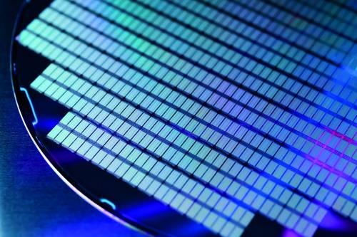
Wide-bandgap semiconductors, such as silicon carbide (SiC),, have long since become a viable alternative to silicon-based devices, especially in power applications, where they can operate at higher voltages, frequencies, and temperatures, providing high reliability and a low cost. This semiconductor material is setting new benchmarks in high-performance electronics development. Silicon Carbide can only be treated with diamond only, due to its exceptional hardness of roughly 2,600 Vickers and its monocrystalline lattice structure. Figure 1 shows a macro photo of a SiC wafer, where each square is a microchip that includes transistors and circuits on a small scale. Individual chips are diced from wafers like this one, which are mainly used for high-power devices, such as MOSFETs, diodes, and power modules.

The steps involved in SiC wafer processing can be summarized as follows:
- multi-wire sawing (MWS)
- double side polishing coarse (DSP)
- double side polishing fine (DSP)
- chemical mechanical polishing (CMP)
This process can be planned and carried out effectively with outstanding results in terms of wafer geometry and surface quality, thanks to Pureon’s innovative, high-quality suspensions made specifically for this purpose. Double-side polishing is one of the major critical steps for the manufacturer, as well as the single-side CMP.
“We are providing our customers the products to make silicon carbide wafer more efficient and economical. The cost of ownership of the process is something that is important to us as it is important to the customer. Right now we are working on the next generation of 200 mm silicon carbide wafer which is going to come sooner or later”, says Bollina.
Diamond suspensions from Pureon for excellent surface finishing
Surface finishing is critical, since it is not possible to use any type of abrasive to get the finish on silicon carbide. The only thing that is harder than silicon carbide is diamond, so we need to use diamond suspensions, and the pad and the diamond suspension combination is a Pureon’s secret recipe. The diamond suspension for the polishing, the pad, and their combination do an excellent surface finish, obtaining a surface roughness of less than five nanometers. That means this process (see Figure 2) achieves an extremely fine surface finish, with a total thickness variation (TTV) of the wafer less than 0.001 micron. This innovative process is highly economical and easily adaptable to customer specifications.

Within this process, reliability is strictly related to consistency. All of the processed wafers shall have the same surface finish, the same material removal rate, and no sub-surface damage. “It is necessary to make sure that the 150 millimeter wafer has as many clean areas as possible, so that you can reduce the loss and increase the area on which you can build the devices. So reliability for us means every single wafer that the customer produces has the same surface finish and the same TTV”, says Bollina.
Lapping and polishing superhard materials with IRINO-PRO-C
Pureon products for SiC wafer processing also include the urethane polishing pad MHN15A and the composite polishing pad IRINO-PRO-C. MH polishing pads are specifically designed for polishing and finishing a wide variety of surfaces where flatness and ultra-precision surface finish is critical, such as semiconductor wafers. By embedding the abrasive into the top surface of the pad, the MH structure maximizes the abrasive’s cutting action while limiting loose particles that can lead to scratching. The novel composite polishing pad IRINO-PRO-C is most suitable for lapping and polishing of superhard materials such as silicon carbide.
What is most important for all its customers is that Pureon can take advantage of a state of the art surface lab, where all the relevant tests and trials for the customers can be performed. All the testing can be done in house, providing the customers with a solution that reduces both the process time as well as the cost of consumables.